Engineering the Future with Diamond.
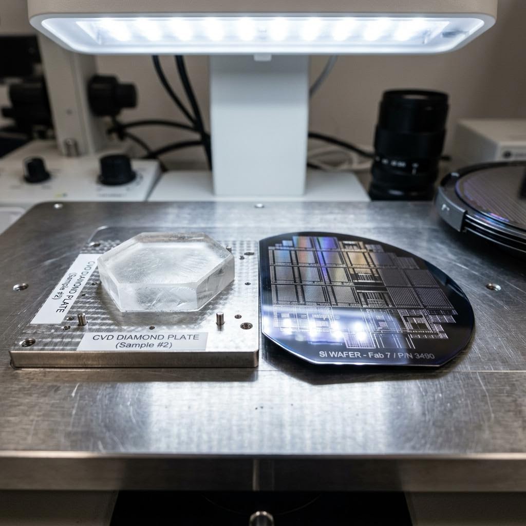
We design and manufacture ultra-pure lab-grown CVD diamond wafers, plates, and composite substrates for semiconductors, quantum computing, and high-power electronics.
Not a Gemstone. A Fundamental Substrate.
Natural diamonds and high-pressure high-temperature (HPHT) synthetic diamonds are plagued by metallic impurities, nitrogen inclusions, and limited sizes, rendering them useless for advanced engineering.
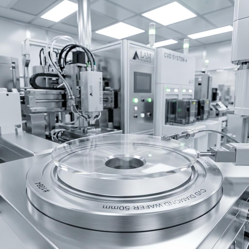
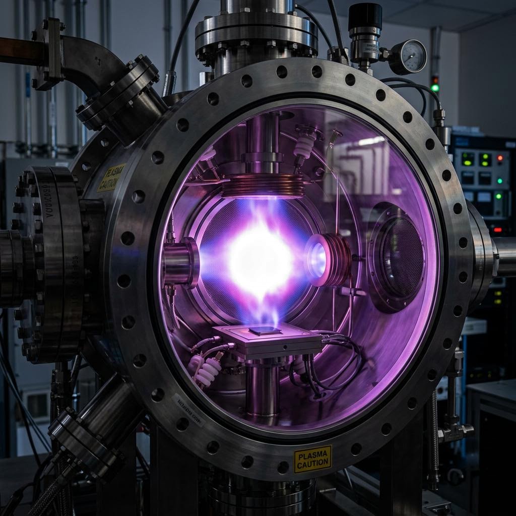
Chemical Vapor Deposition (CVD) changes the paradigm. We grow diamond atom-by-atom in a high-vacuum plasma environment. This allows us to precisely control dopants, eliminate impurities to parts-per-billion levels, and scale wafer sizes up to 8 inches.
- Isotopic purity for extended quantum coherence
- Custom doping profiles (Boron, NV centers)
- Sub-nanometer surface roughness via CMP
Unrivaled Physical Properties
No other material simultaneously possesses extreme thermal conductivity, broad optical transparency, and exceptional dielectric strength.
Extreme Thermal Management
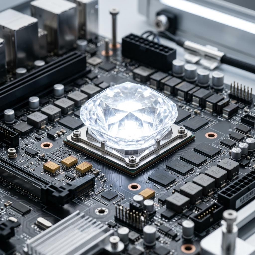
Diamond has the highest thermal conductivity of any known material, making it the ultimate heat sink for high-power chips and laser diodes.
Unmatched Dielectric Strength
Outstanding electrical insulation capabilities allow for smaller, more efficient high-voltage devices and next-gen power electronics.
Quantum-Grade Purity
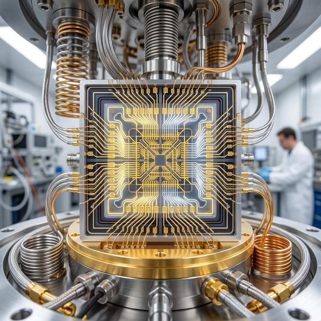
Nitrogen-Vacancy (NV) centers in our ultra-pure single-crystal diamond serve as the foundation for room-temperature quantum computing.
Radiation Hardness
Inherently resistant to radiation, making our diamond substrates ideal for aerospace, defense, and deep-space applications.
Semiconductor Integration
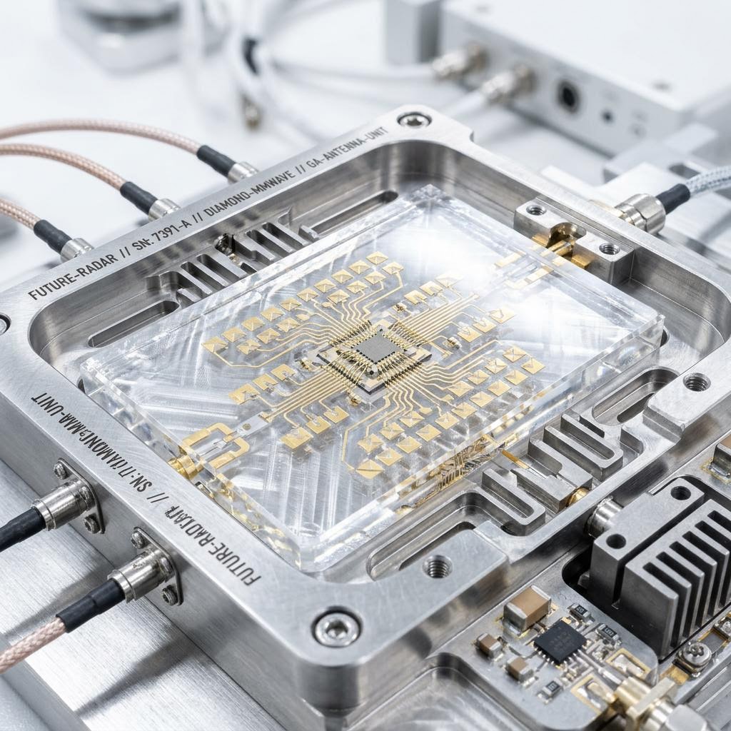
We engineer composite substrates (GaN-on-Diamond) to bring the thermal benefits of diamond directly to wide-bandgap semiconductors.
Optical Transparency
Exceptional transmission from deep UV to far infrared wavelengths, perfect for high-power laser windows and advanced optics.
Breaking the Silicon Thermal Barrier
Modern processors and RF amplifiers generate massive heat densities. Copper and Aluminum Nitride heat spreaders can no longer keep up, creating thermal bottlenecks that throttle performance. CVD Diamond provides an immediate, radical performance leap.

Engineered Materials Catalog
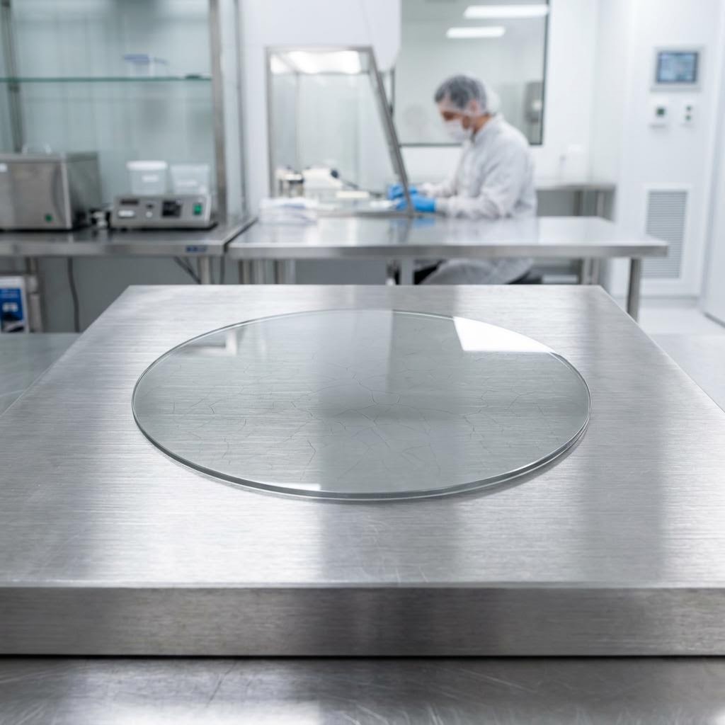
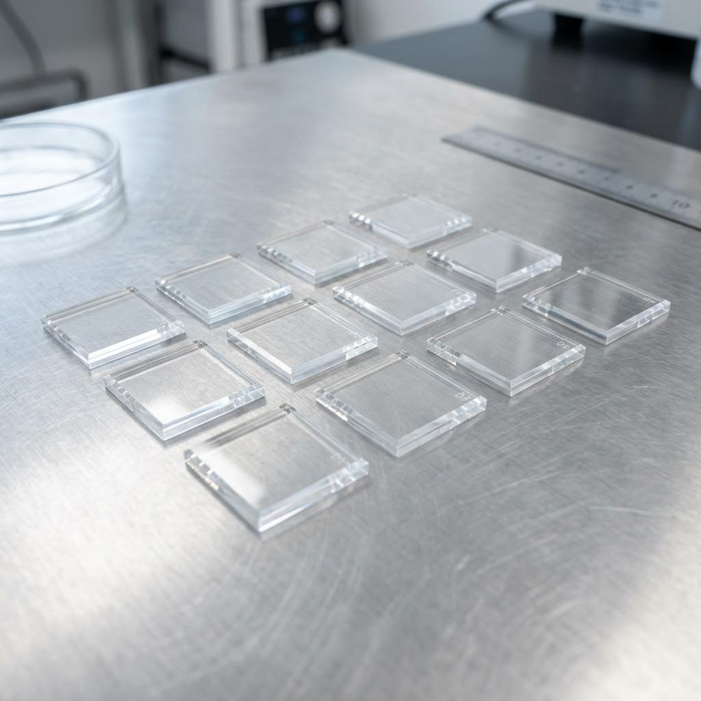
Off-the-shelf and custom-grown diamond wafers for integration into existing manufacturing pipelines.
Inside the CVD Reactor
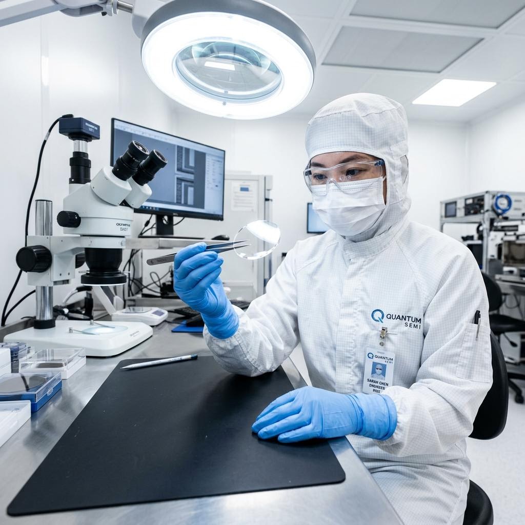
We recreate the extreme conditions of a dying star inside Class 1,000 cleanrooms, growing perfect diamond lattice structures atom by atom.
Discover Our ProcessPowering Next-Gen Industries
When silicon, copper, and sapphire fail under extreme loads, the world's most advanced sectors turn to diamond.

Certified for the Extremes
Our manufacturing facilities adhere to strict defense, aerospace, and commercial quality standards. Every wafer ships with a comprehensive metrology report certifying its crystalline purity and thermal performance.
Subscribe to Our Newsletter
Stay updated on the latest advancements in CVD diamond materials, manufacturing breakthroughs, and industry applications.