Engineered Products
A comprehensive portfolio of precision-engineered diamond wafers, plates, and composites. Ready for direct integration into your manufacturing pipeline or custom-grown to your exact specifications.
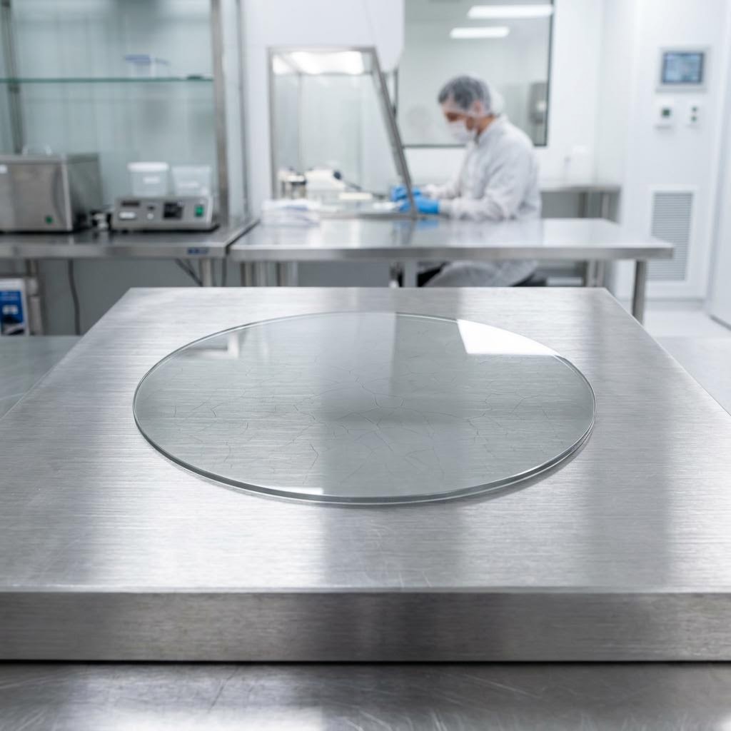
Thermal Grade Polycrystalline CVD Diamond
Engineered specifically for extreme heat spreading applications, our Thermal Grade Polycrystalline CVD Diamond offers an unparalleled combination of thermal conductivity and large-area scalability. Grown in proprietary microwave plasma reactors, these wafers are devoid of the metallic binders found in HPHT diamonds. They act as the ultimate heat sink for high-power electronics, laser diode arrays, and dense computing architectures, allowing devices to operate at significantly higher power levels without thermal degradation.
Specs & Tolerances
- Thermal Conductivity: 1000 - 2000 W/m·K
- Dielectric Constant: 5.7
- Electrical Resistivity: > 10¹³ Ω·cm
- Surface Roughness (Ra): < 10nm (after CMP)
Material Properties
- Isotropic thermal properties across the wafer
- Chemically inert and biocompatible
- Exceptional mechanical strength and hardness
Key Advantages
- Reduces junction temperatures in high-power chips
- Allows for massive increases in component packing density
- Eliminates the need for bulky, active cooling systems
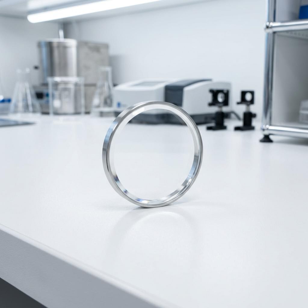
Optical Grade Polycrystalline CVD
Designed for applications requiring maximum light transmission across a broad spectrum, our Optical Grade Polycrystalline Diamond is synthesized with an extremely low nitrogen content. This results in a material with exceptional transparency from the deep ultraviolet to the far infrared and microwave bands. It is the material of choice for high-power CO2 laser windows, multispectral imaging systems, and gyrotron windows where both optical clarity and thermal shock resistance are mandatory.
Specs & Tolerances
- Optical Transmission: > 70% @ 10.6μm (uncoated)
- Absorption Coefficient: < 0.05 cm⁻¹ @ 10.6μm
- Thermal Shock Parameter: 10⁷ W/m
- Refractive Index: 2.38
Material Properties
- Broadband optical transparency
- Immune to thermal shock fracturing
- Highly resistant to abrasive and corrosive environments
Key Advantages
- Enables higher power output in industrial lasers
- Reduces optical distortion caused by thermal lensing
- Protects sensitive sensor payloads in harsh environments
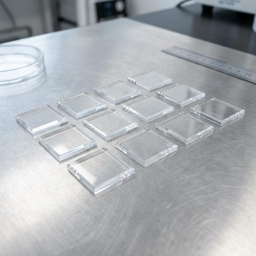
Electronic Grade Single-Crystal Diamond
For the most demanding active semiconductor applications, grain boundaries are unacceptable. Our Electronic Grade Single-Crystal Diamond plates are grown via a highly controlled homoepitaxial CVD process, resulting in a virtually defect-free lattice. With ultra-low impurity levels of nitrogen and boron, these plates provide the highest possible charge carrier mobility, making them ideal for high-power, high-frequency RF devices, high-voltage switches, and extreme-environment detectors.
Specs & Tolerances
- Nitrogen Concentration: < 5 ppb
- Dislocation Density: < 10⁴ cm⁻²
- Electron Mobility: > 3800 cm²/V·s
- Hole Mobility: > 3000 cm²/V·s
Material Properties
- Zero grain boundaries
- Maximum theoretical thermal conductivity (>2200 W/m·K)
- Ultra-wide bandgap (5.45 eV)
Key Advantages
- Enables true diamond-based active electronics
- Supports massive breakdown voltages for power grids
- Flawless performance in high-radiation environments
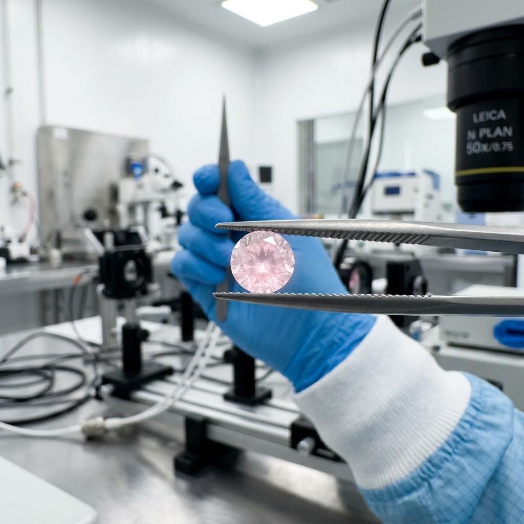
Quantum Grade Single-Crystal Diamond
The backbone of the coming quantum revolution. Nanomine's Quantum Grade Diamond is meticulously engineered to host Nitrogen-Vacancy (NV) centers—precise atomic defects that function as robust qubits. By utilizing isotopically purified Carbon-12 during the CVD growth phase, we eliminate the nuclear spin interference caused by Carbon-13 isotopes. This results in incredibly long spin coherence times at room temperature, paving the way for scalable quantum computers and ultra-sensitive magnetic and electric field sensors.
Specs & Tolerances
- NV Center Concentration: Custom (1 ppb to 10 ppm)
- Carbon-12 Isotopic Purity: > 99.999%
- Spin Coherence Time (T2): > 2ms at room temp
- Orientation: (100) or (111) available
Material Properties
- Stable, optically addressable spin states
- Extremely low magnetic noise environment
- Room-temperature quantum operation
Key Advantages
- Eliminates the need for cryogenic cooling for qubits
- Enables highly sensitive nanoscale magnetometry
- Provides a reliable, solid-state platform for quantum networks
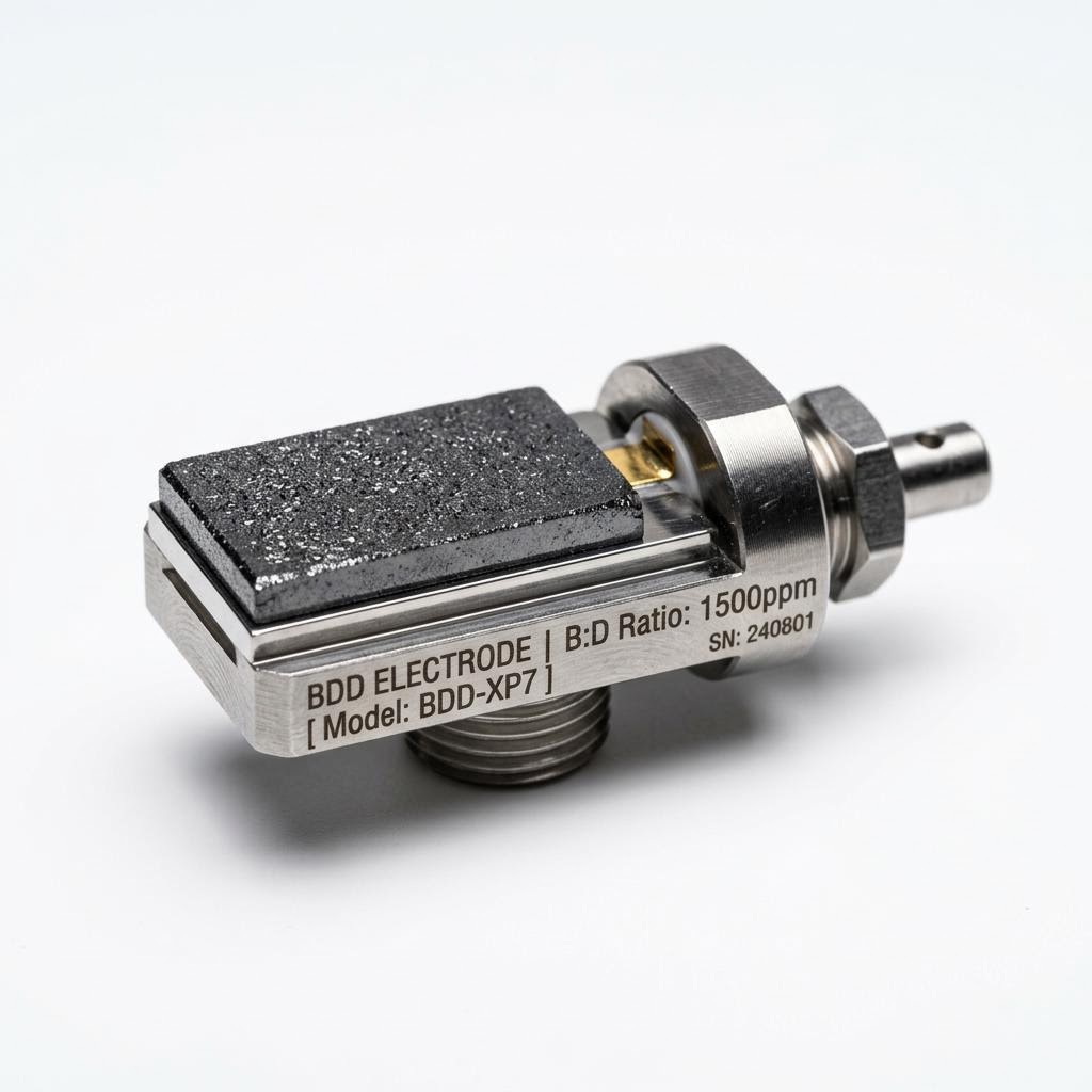
Boron-Doped Diamond (BDD)
By intentionally introducing boron gas during the CVD growth process, we transform diamond from a perfect insulator into a highly conductive electrode material. Boron-Doped Diamond (BDD) possesses the widest electrochemical potential window of any known electrode material, combined with total chemical inertness. This makes it a revolutionary component for advanced wastewater treatment (generating hydroxyl radicals to destroy PFAS/forever chemicals), electrochemical sensing, and severe-environment electrosynthesis.
Specs & Tolerances
- Boron Doping Level: 100 to 10,000 ppm
- Electrical Resistivity: 0.1 to 0.001 Ω·cm
- Potential Window: ~3.5 V in aqueous solutions
- Background Current: Extremely low
Material Properties
- Metallic-level electrical conductivity
- Complete resistance to corrosive acids and bases
- Resistant to bio-fouling and scaling
Key Advantages
- Destroys complex organic pollutants efficiently
- Lasts orders of magnitude longer than lead-oxide electrodes
- Provides highly accurate electrochemical sensing metrics
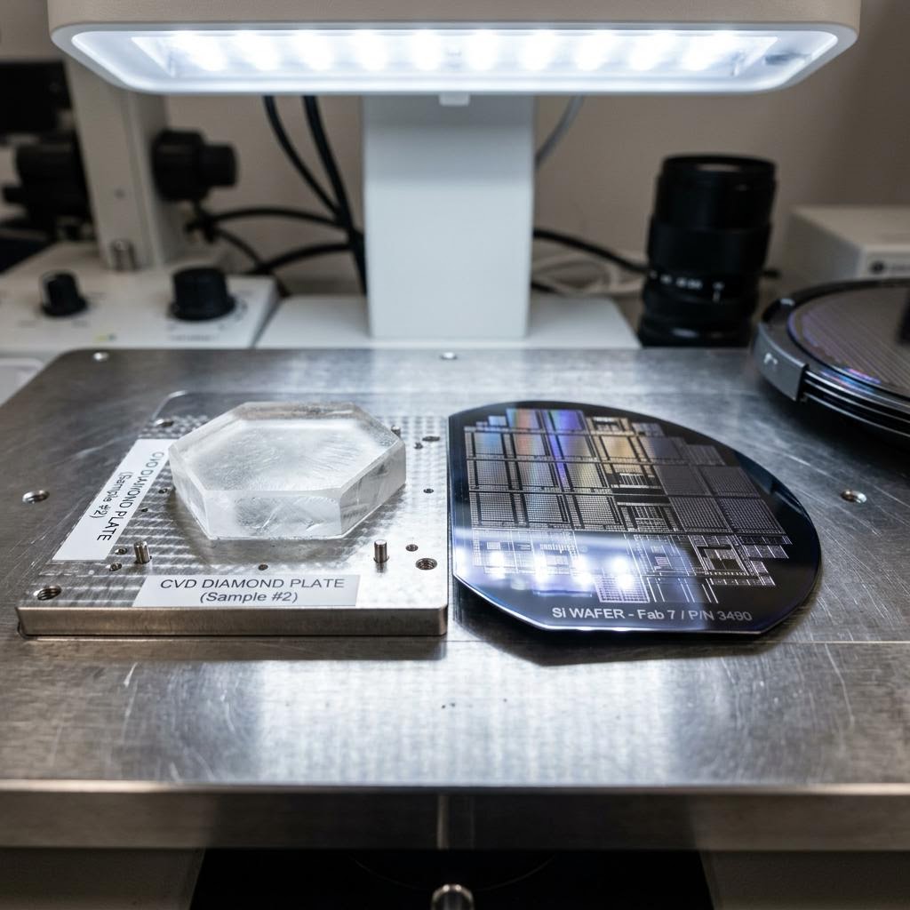
GaN-on-Diamond / Diamond & Copper Composite Wafers
Gallium Nitride (GaN) HEMTs are the standard for high-power RF communications, but their power density is fundamentally capped by the poor thermal conductivity of their underlying silicon or SiC substrates. Nanomine's GaN-on-Diamond and Diamond-Copper technology solves this by chemically bonding high-conductivity heat spreaders directly to power modules. This intimate contact removes the thermal bottleneck, allowing RF devices in 5G/6G base stations and military radars to operate at power levels previously thought impossible.
Specs & Tolerances
- Epitaxial Layer: Standard AlGaN/GaN HEMT structure
- Diamond Thermal Conductivity: > 1500 W/m·K
- Thermal Boundary Resistance: < 10 m²·K/GW
- Wafer Bow: < 30μm
Material Properties
- Combines GaN/Copper's traits with Diamond's thermal traits
- Minimizes distance between heat generation and heat sink
- Stress-managed composite interface
Key Advantages
- Increases max power density by up to 300%
- Reduces overall device size and weight
- Extends the operational life of base station amplifiers
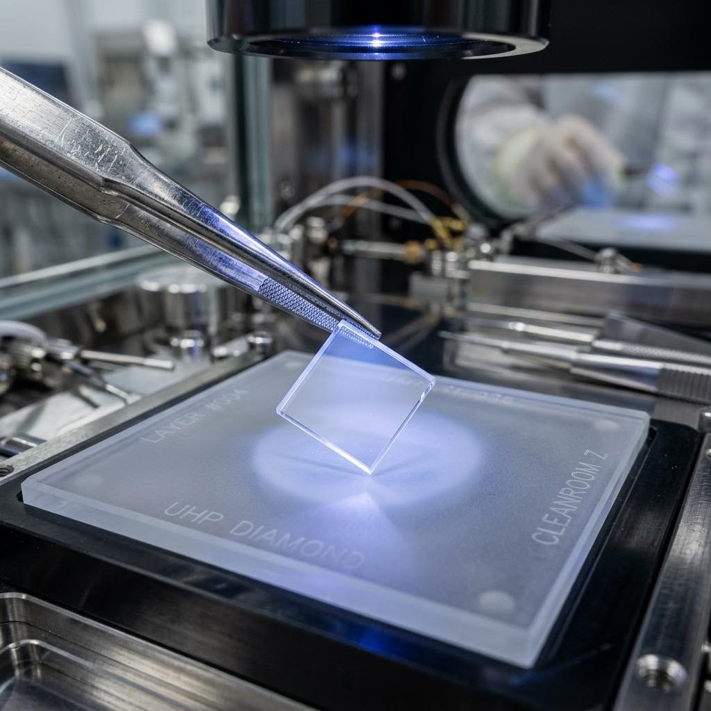
Ultra-High Purity Epitaxial Layers
For clients developing proprietary semiconductor architectures, we offer ultra-high purity diamond epitaxial deposition services. We grow defect-free, single-crystal diamond layers directly onto client-provided diamond seeds or specific engineered substrates. With atomic-level control over the plasma chemistry, we achieve pristine crystalline growth tailored for advanced R&D in solid-state physics, deep-UV LEDs, and experimental high-power diodes.
Specs & Tolerances
- Impurity Levels: Sub-ppb for N and B
- Growth Rate: Highly controlled for lattice perfection
- Surface Finish: As-grown or CMP polished
- Raman FWHM: < 1.5 cm⁻¹
Material Properties
- Flawless continuation of seed crystal lattice
- Customizable doping profiles layer-by-layer
- Extreme purity for specialized research
Key Advantages
- Provides a blank canvas for custom device fabrication
- Enables multi-layer diamond semiconductor designs
- Accelerates institutional R&D timelines