About Nanomine
We are materials scientists, plasma physicists, and engineers united by a single vision: to overcome the physical limitations of legacy materials through the industrialization of CVD diamond.
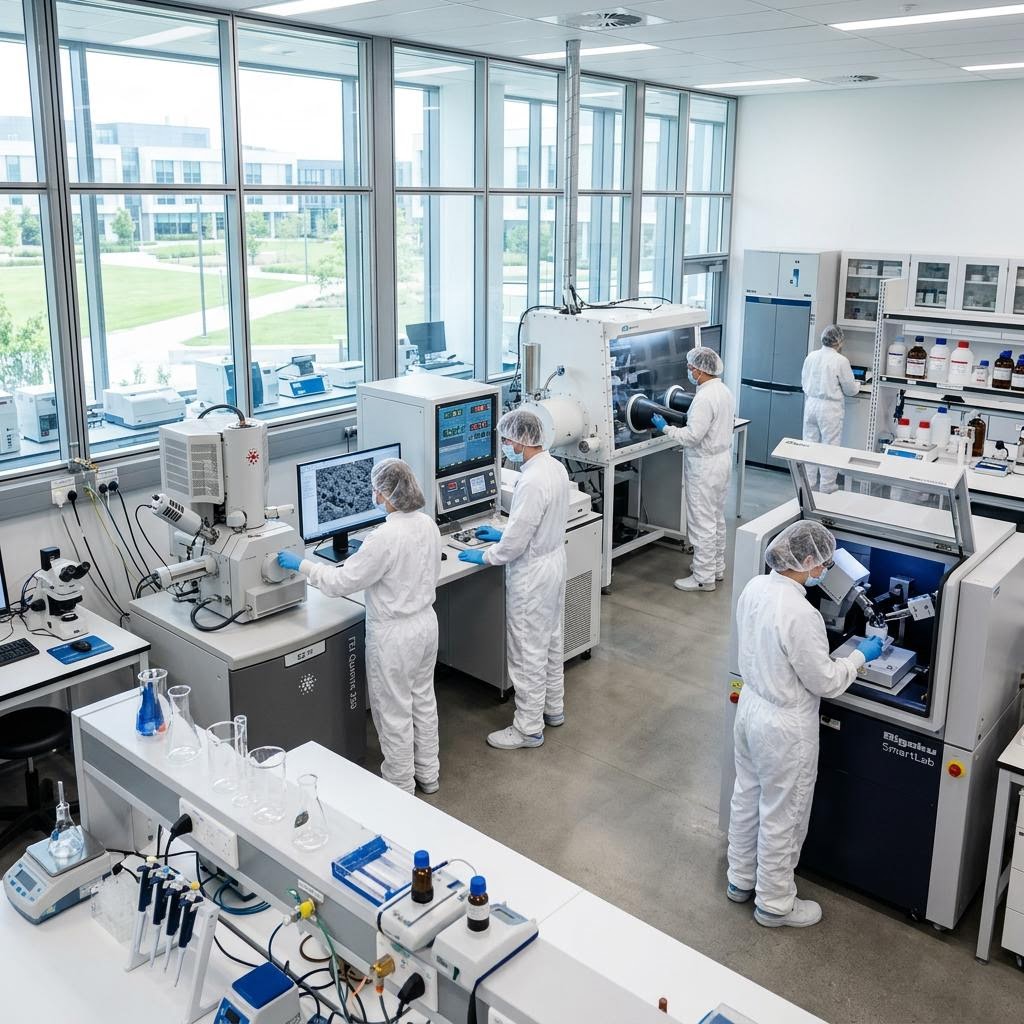
Our Origin & Mission
Founded in Silicon Valley by veterans of the semiconductor industry, Nanomine Techno Labs was built to solve a looming crisis: computational hardware was burning up. Copper and silicon carbide were no longer enough to handle the thermal density of modern GPUs and RF amplifiers.
Our mission is to engineer, manufacture, and deliver the highest quality lab-grown CVD diamond substrates in the world. We don't make jewelry; we manufacture the foundational substrate for the next generation of extreme-performance electronics, quantum networks, and deep-space arrays.
Experience the Difference
What sets Nanomine apart is our obsession with control. From custom-building our microwave plasma reactors to formulating proprietary hydrogen/methane gas recipes, we own the entire growth cycle.
This vertical integration allows us to achieve impurity levels measured in parts-per-billion and scale wafer diameters to sizes previously thought impossible. When prime defense contractors and hyper-scale data centers need a material that simply will not fail under stress, they choose Nanomine.
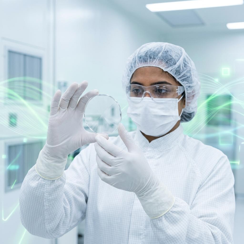
Engineering for Sustainability
Industrial advancement cannot come at the cost of environmental degradation. Traditional semiconductor materials often require massive, environmentally destructive mining operations.
Nanomine's CVD process produces a vastly superior material using only electricity, methane, and hydrogen inside a closed-loop laboratory environment. Furthermore, the very products we manufacture—extreme heat spreaders and power electronics substrates—directly enable the global transition to high-efficiency electric vehicles and drastically reduce the massive energy consumption of modern data centers.
Our Core Values
The principles that govern our laboratories, our boardrooms, and our engineering decisions.
Integrity
Uncompromising honesty in our engineering data, reporting, and client relations.
Customer Focus
Developing bespoke materials perfectly tailored to solve exact client bottlenecks.
Innovation
Constantly pushing the boundaries of plasma physics and materials science.
Collaboration
Partnering deeply with prime contractors, academia, and research institutions.
Sustainability
Pioneering highly efficient growth processes to reduce our energy footprint.
Respect
Fostering a culture of safety, inclusivity, and technical excellence in our labs.
Quality
Adhering to strict AS9100D and ISO metrics; if it isn't perfect, it doesn't ship.